The electronics industry is approaching a limit to the number of transistors that can be packed onto the surface of a computer chip. So, chip manufacturers are looking to build up rather than out.
Instead of squeezing ever-smaller transistors onto a single surface, the industry is aiming to stack multiple surfaces of transistors and semiconducting elements — akin to turning a ranch house into a high-rise. Such multilayered chips could handle exponentially more data and carry out many more complex functions than today’s electronics.
A significant hurdle, however, is the platform on which chips are built. Today, bulky silicon wafers serve as the main scaffold on which high-quality, single-crystalline semiconducting elements are grown. Any stackable chip would have to include thick silicon “flooring” as part of each layer, slowing down any communication between functional semiconducting layers.
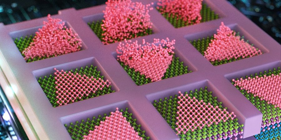
Now, MIT engineers have found a way around this hurdle, with a multilayered chip design that doesn’t require any silicon wafer substrates and works at temperatures low enough to preserve the underlying layer’s circuitry.


