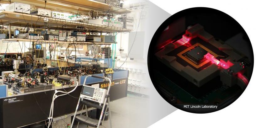
Breakthroughs in quantum technologies for computing, sensing, and communications can take decades to transition from laboratory to real-world use. This is, in part, due to the need for extensive laboratory setups to maintain the highly delicate quantum states of atoms, which very quickly lose coherence (i.e., their “quantumness”) when disturbed by the slightest interference of sound, heat, or light.
Advances in chip-scale electronics — such as nanophotonic lasers (fractions of a millimeter in size), compact high-speed cameras, and feedback circuitry — could potentially replace today’s large, expensive lab equipment, enabling faster development of low size, weight, and power quantum devices. A major roadblock, however, is the inability to test and certify the performance of these miniaturized technologies against their quantum laboratory counterparts.
DARPA’s Optical-Atomic System Integration & Calibration (OASIC) program, a Small Business Technology Transfer (STTR) effort, aims to develop advanced quantum testbeds that rapidly test, evaluate, and prototype integrated chip-scale quantum technologies for practical use. These state-of-the-art quantum testing centers are envisioned as fee-based facilities open to any users in the technical community to evaluate their components against the best laboratory-based quantum bits (qubits), quantum sensors, and atomic clocks.


